
Recently, I designed a small piece of hardware with the ESP32-S2 chip, but there are problems in the antenna circuit design. I hope to give some guidance, such as layout rules and how to match the Π-type network.
I made some modifications and optimizations for the V1 and V2 of the PCB. The following is the design of the V3 of the board, I hope the engineer or Daniel can help to see if the current design is OK.
Schematic diagram:
PCB layout diagram:
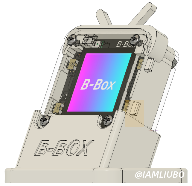
3D view:
Using a 2.4G ceramic antenna, the current problems are:
1. Whether the current layout meets basic usage (requirements are not so high)
2. How to calculate the capacitance and inductance in the Π matching network
3. Whether the ceramic antenna can meet the design
Because this small project is designed and played by itself, there is no particularly high requirement for the antenna, and it can be basically used. The module was initially considered, but due to the large size, it has to start with the chip. There are two versions of the PCB, and there are no problems with other parts except the antenna, so this time I want to take care of the antenna part.
Thank you.
IAMLIUBO