
I have a PCB that requires a ESP32-DevKitC. My circuit and PCB have just the 2 rows of 19 pins THT connectors. I buy the PCB from JLCPCB with all the surface stuff mounted, but I have to hand solder the 2 19pin THT connectors and then plug in my DevKitC.
What's the easiest way to effectively take the DevKitC schematic and plop it onto my pcb so the ESP32 is SMT right onto my PCB? Is there a reference design I can just use?
I am investigating how to make this design more manufacturable. Ideally my design could be ordered from JLCPCB with the ESP32 soldered for me. JLCPCB will assemble the SMT ESP32-PICO-D4. Is there a reference circuit that effectively duplicates the functionality of the DevKitC with the PICO include the socket for an antenna?
Ideally, I will also eliminate the power supply in the process. I have my own 3.3V regulated power supply for my board, so I don't see why I need to have the power stuff from the DevKitC design. Is there a reference design I can copy where there is no USB and no power supply but there is a 2x3 header where you plug something like the Micro Pro Avr Tiny ISP in to supply the 3.3 and program it?
A separate but related question is whether there is an ESP32 variant that has over the air programming? I assume the chip would have some ROM that will boot the thing in AP mode and accept a sketch. That type of solution, preferably with a reference circuit that I can use, would eliminate the need for the USB and power stuff that's probably the bulk of the DevKitC thing.
Thanks in advance, and I apologize for failing to find the answer myself.
How to create circuit/pcb to eliminate dev board
Re: How to create circuit/pcb to eliminate dev board
Sounds like you're already using schematic and PCB layout software, that's good.
The "reference design" to "plop it onto" your PCB I would say is simply the schematic of the DevKit itself: https://dl.espressif.com/dl/schematics/ ... v4-sch.pdf
Especially since you are saying "take out the power supply, take out the USB connector and serial chip", there isn't much left of the DevKitC board. You're basically just using the ESP32-PICO-D4.
In my workflow, I use EasyEDA for schematic and PCB layout, and I use LCSC as much as possible for a component supplier. If LCSC doesn't have it I go to digikey or mouser, but the leadtime will likely be a bit higher for a SMT / PCBA service company in China.
You would look up the parts one by one from the schematic you're copying, find the part in LCSC, and place it into your schematic in easyeda. You'll have to pick specific parts based on what's in stock and price. And you'll have to route the PCB.
This is very common in schematic/PCB work, you copy from other circuits that are in datasheets or other shared schematics. You'll very often have to "recreate" it for your own PCB, so it's worthwhile to get good at it.
There are tons of PCBA service companies other than JLCPCB. JLCPCB has done a good job making it easy to order, but they are somewhat limited in which parts they will populate on your board, this ends up limiting your designs and requiring a lot of hand soldering by you. Personally, I use PCBWAY, they have pretty good service and pricing. It is very similar to JLCPCB, you just export your gerber and BOM files, and upload those on the pcbway website.
You can send me a PM if you'd like to work together on doing schematic and board layout.
Yes ESP32 has OTA programming. I have not used it yet myself.
https://randomnerdtutorials.com/esp32-o ... ogramming/
I believe you still need a way to "hard wire" program it for the initial setup, because you need to upload the wifi credentials to get it on your network. After it's network connected, then you can do OTA. Your board could have a small JTAG 1x4 pin header, this connects to VDD GND TX RX on the ESP32. (If you want auto flash, 2 more pins for GPIO0 and RESET). Then you have a separate programmer board with the usb connector, usb to serial chip, and 3.3V power supply. This can shift the bulk of that one-time setup stuff off of your main board. Here is a board I made you can use as a reference for that: https://easyeda.com/coreymberman/esp32-programmer
Re: How to create circuit/pcb to eliminate dev board
You may want to choose a shielded module if you want to reuse rf certifications
Re: How to create circuit/pcb to eliminate dev board
Thanks for the feedback.
I have been using easyda and have experienced your point about part availability. I will look into PCBWAY. Will they mount THT parts?
I think I am getting quite proficient at banging out PCBs. I don't really have the experience to know what I am clueless about with respect to noise and other non binary stuff. But in general my circuits have functioned properly. I did make some version that sucked when my inverter had a load. I think was solved by eliminating a ground loop. I don't know if my design would survive some noisy environment though. Or to be blunt, whenever the reference circuit has some capacitor or inductor across something, I assume it is filtering noise, but I have no intuition to have placed it there in the first place.
The reference circuit you referred me to has the WROOM or WROVER, how does that relate to the PICO? At a glance, the WROOM and WROVER have the antenna, but it also seems like they might have RAM or EEPROM? If so, then maybe the WROOM/WROVER (I have not figured out the difference yet) would be easier, but then I'd have to figure out how to mount it to the PCB. Is there a socket for it? Is the module just SMT? Can I hand solder that? Sorry, I am confused between what is an ESP32 and the WXXX's and PICO.
If I get rid of the Micro USB 5V&USB-UART section, how I am programming the thing? My bet is that I can bring out 6 pins to a 2x3 .1" connector and then I plop a common usb -> 2x3 thingy that I have that I use to program an attiny. But any short cuts to that solution would be greatly appreciated.
With respect to OTA. I would want a solution where if the burn somehow craps out, the user just holds some reset button for n Secs, which resets some EPROM and now the thing boots factory. In that factory mode, the software would fire up the WiFi in AP mode to accept the new software. Is that possible?
Re: How to create circuit/pcb to eliminate dev board
I think I do care about rf certification. Thanks for bringing that up.
Am I correct to understand that the modules that have the antenna and metal cover over the chip have that rf cert?
Is that the difference between a PICO chip and a WROOM/WROVER type module?
Am I correct to understand that the modules that have the antenna and metal cover over the chip have that rf cert?
Is that the difference between a PICO chip and a WROOM/WROVER type module?
Re: How to create circuit/pcb to eliminate dev board
If you are trying to sell this commercially as an end product, the RF certification matters. The WROOM / WROVER modules are precertified. If you use an ESP32 chip or ESP32-PICO, you would probably have to pay $1000's for RF certification testing on your end product.
https://www.reddit.com/r/esp32/comments ... icod4_fcc/
Yes PCBWAY would do THT parts. It might increase your cost a bit b/c it is more labor to place THT parts. Usually its people sitting at benches taking the parts from bins and putting them on, vs a pick and place machine for SMT. (that's how any PCB house would do it, not just pcbway)
You can hand solder a WROOM/WROVER module pretty easily. The pins are all castellated holes you can fit a solder tip right onto. You will need an exposed ground pad on the bottom side of the board to get the ground pad soldered in the center of the module, applying heat from the bottom / opposite side of the pcb.
https://www.youtube.com/watch?v=wQip1PhYW34
Take some time reading through the datasheets to understand the PICO, WROOM, and WROVER. They are modules that integrate an ESP32 chip (the MCU), plus the crystal oscillator, plus some flash memory, plus some impedance matching for the antenna. They are really similar pin-to-pin, as far as how you use them electrically. The main benefit of the PICO is that it is the smallest SiP integrating all that stuff for you, it is barely larger than an ESP32 chip itself. The main benefit of the WROOM / WROVER is the RF certification and the fact all the antenna RF stuff is already done for you. (With PICO it is still pretty easy to add a chip antenna)
ESP32-PICO opened up, you can see the crystal, small components, and flash memory, integrated on top of the chip:

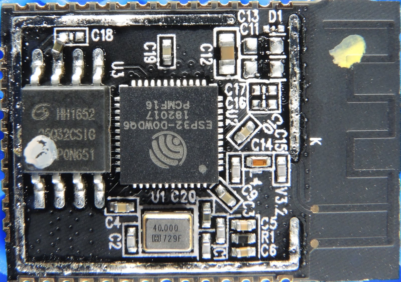
WROOM with the shield removed. You can directly see the ESP32-D0WDQ6 chip, the flash memory, the crystal, bypass caps, impedance matching components, and the PCB trace antenna.
https://www.espressif.com/sites/default ... eet_en.pdf
Go to page 19 for the schematic:
https://www.espressif.com/sites/default ... eet_en.pdf
You could probably implement this 5-second reset thing for your end users. You might need a separate memory chip that holds your desired "factory" image, and some other circuitry that detects the reset button and begins reflashing the esp32 with your custom image, that could be pretty cool. But you yourself would still need the physical serial connection for the very first time you get this stuff programmed.
https://lastminuteengineers.com/esp32-o ... duino-ide/
Read the espressif docs on OTA for the most direct info about it:
https://docs.espressif.com/projects/esp ... m/ota.html
https://www.reddit.com/r/esp32/comments ... icod4_fcc/
Yes PCBWAY would do THT parts. It might increase your cost a bit b/c it is more labor to place THT parts. Usually its people sitting at benches taking the parts from bins and putting them on, vs a pick and place machine for SMT. (that's how any PCB house would do it, not just pcbway)
You can hand solder a WROOM/WROVER module pretty easily. The pins are all castellated holes you can fit a solder tip right onto. You will need an exposed ground pad on the bottom side of the board to get the ground pad soldered in the center of the module, applying heat from the bottom / opposite side of the pcb.
https://www.youtube.com/watch?v=wQip1PhYW34
Take some time reading through the datasheets to understand the PICO, WROOM, and WROVER. They are modules that integrate an ESP32 chip (the MCU), plus the crystal oscillator, plus some flash memory, plus some impedance matching for the antenna. They are really similar pin-to-pin, as far as how you use them electrically. The main benefit of the PICO is that it is the smallest SiP integrating all that stuff for you, it is barely larger than an ESP32 chip itself. The main benefit of the WROOM / WROVER is the RF certification and the fact all the antenna RF stuff is already done for you. (With PICO it is still pretty easy to add a chip antenna)
ESP32-PICO opened up, you can see the crystal, small components, and flash memory, integrated on top of the chip:
WROOM with the shield removed. You can directly see the ESP32-D0WDQ6 chip, the flash memory, the crystal, bypass caps, impedance matching components, and the PCB trace antenna.
https://www.espressif.com/sites/default ... eet_en.pdf
Go to page 19 for the schematic:
https://www.espressif.com/sites/default ... eet_en.pdf
You will need to make a serial (physical) connection for that first upload, going from factory image to having some code that tells it to accept OTA programming. After that, you can do OTA. If something goes wrong and the esp32 needs to be reflashed, you probably need the physical serial connection again. So for all those reasons, you always need some pins available to make a serial connection to your board. You can place a tiny 1x6 or 2x3 pin header to achieve this.With respect to OTA. I would want a solution where if the burn somehow craps out, the user just holds some reset button for n Secs, which resets some EPROM and now the thing boots factory. In that factory mode, the software would fire up the WiFi in AP mode to accept the new software. Is that possible?
You could probably implement this 5-second reset thing for your end users. You might need a separate memory chip that holds your desired "factory" image, and some other circuitry that detects the reset button and begins reflashing the esp32 with your custom image, that could be pretty cool. But you yourself would still need the physical serial connection for the very first time you get this stuff programmed.
https://lastminuteengineers.com/esp32-o ... duino-ide/
https://randomnerdtutorials.com/esp32-o ... ogramming/The factory image in ESP32 doesn’t have an OTA Upgrade capability. So, you need to load the OTA firmware on the ESP32 through serial interface first.
It’s a mandatory step to initially update the firmware, so that you’re able to do the next updates/uploads over-the-air.
Read the espressif docs on OTA for the most direct info about it:
https://docs.espressif.com/projects/esp ... m/ota.html
Re: How to create circuit/pcb to eliminate dev board
Hi, Becorey.
Your posts were useful to me since I am intending to launch products not based on a development board, although it would be a comfortable choice in some aspects.
My no more existing doubt was related to code upload to an ESP32 module (probably a WROOM-32 one), but the programmer circuitry published at https://easyeda.com/coreymberman/esp32-programmer that has cleared it all. There are many very cheap USB-serial converters on the market, so uploading code is not a problem anymore.
According ESP32-WROOM-32 datasheet (https://www.espressif.com/sites/default ... eet_en.pdf), if I have not got it wrong, I´ll only need a 3.3V power supply and some specific PCB design to make things work and even a 2-layer PCB will be enough.
I intend to use ESP32-WROOM-32 in a very electrically polluted application. Would you know some ESP32-specific vulnerability related to this kind of environment?
Re: How to create circuit/pcb to eliminate dev board
Did you succeed?
The most comprehensive introduction to shipping from China to the UAE in 2023. https://www.dantful.com/news/industry-n ... -2023.html
Who is online
Users browsing this forum: No registered users and 64 guests